
The Role of Semiconductor Optics: Laser and Imaging Technologies in Semiconductor Equipment
Author: Bryan Ng – Marketing Manager
Published on:
Last edited:

Semiconductor manufacturing processes rely heavily on precise optical systems to achieve the required resolution, accuracy, and efficiency. Among the most critical optical technologies in this domain are laser optics and imaging optics, which are integral to the functioning of advanced semiconductor equipment. These systems enable everything from wafer inspection and defect detection to the high-precision processing of semiconductor materials. As the demand for smaller and more powerful semiconductor devices increases, laser and imaging optics continue to evolve, pushing the boundaries of optical performance and precision.
1. Laser Optics in Semiconductor Processing
Laser optics play a pivotal role in semiconductor processing, enabling a wide range of applications that demand exceptional accuracy and control. These optical systems are designed to manipulate laser beams with high precision, delivering concentrated energy exactly where it’s needed. This capability is crucial for advanced manufacturing processes such as photolithography, laser etching, thin-film deposition, micromachining, and wafer dicing.
The inherent properties of lasers—such as high beam quality, coherence, and tunable wavelength—combined with the precision alignment and focusing capabilities of advanced optics, make them indispensable tools in semiconductor fabrication. Furthermore, integrating adaptive optics and beam shaping technologies enhances process flexibility and throughput, supporting the production of ever-smaller and more powerful electronic components.
1.1 Laser Etching and Ablation

In semiconductor manufacturing, laser ablation has emerged as a critical technique for high-precision patterning and etching processes. Among the various types of laser sources, femtosecond lasers are particularly valued for their ability to ablate materials with exceptional accuracy and minimal collateral damage. These ultrafast lasers emit pulses in the femtosecond range (10⁻¹⁵ seconds), enabling precise removal of material in thin layers while preserving the structural integrity of the underlying substrate.
The key advantage of femtosecond lasers lies in their “cold ablation” mechanism. Because the pulse duration is shorter than the time it takes for heat to diffuse into the surrounding material, there is negligible thermal effect, drastically reducing the risk of microcracks, melting, or unwanted deformation. This makes them ideal for working with delicate semiconductor materials such as silicon, gallium arsenide, and various compound semiconductors, especially in the fabrication of microelectromechanical systems (MEMS), photonic devices, and advanced integrated circuits.
To achieve the required precision and uniformity, laser optics and beam-shaping components are integrated into the ablation system. These may include spatial light modulators (SLMs), diffractive optical elements (DOEs), f-theta scan lenses, and beam expanders, all of which help tailor the beam profile and focus spot size. This level of beam control ensures uniform energy delivery across the target area, enabling sub-micron resolution and high reproducibility, even in complex multi-layer structures.
1.2 Laser-Induced Chemical Vapor Deposition (LCVD)
Laser-Induced Chemical Vapor Deposition (LCVD) is an advanced material deposition technique that leverages the precision of laser optics to initiate and control localized chemical reactions for the formation of thin films on semiconductor substrates. Unlike conventional chemical vapor deposition (CVD) methods, which rely on uniformly heating the entire substrate, LCVD utilizes focused laser energy to selectively activate chemical precursors, enabling site-specific deposition with unmatched spatial resolution.
In this process, a laser beam is directed onto the surface of a substrate within a chamber filled with reactive precursor gases. The laser’s optical energy is absorbed either by the substrate or directly by the gas-phase molecules, triggering thermally driven or photolytic chemical reactions at the laser’s focal point. This leads to the formation of solid material only in the irradiated zone, allowing precise patterning without the need for masks or post-deposition etching.
The role of laser optics in LCVD is critical. High-power, high-precision optics such as beam shaping modules, focusing lenses, and adaptive optics are employed to control the laser beam’s intensity, spot size, and spatial profile. These components ensure the energy is delivered exactly where it’s needed, with minimal loss or scattering. In many systems, f-theta lenses or telecentric lenses are used to maintain a consistent focal spot across a scanning area, allowing for uniform film deposition even during dynamic processes.
One of the key advantages of LCVD is its ability to deposit films with micron- to sub-micron-scale precision, both in lateral resolution and film thickness. This makes it ideal for applications requiring selective material growth, such as microelectronics, photonic devices, micro-opto-electromechanical systems (MOEMS), and repairing g defects in semiconductor patterns. Additionally, LCVD enables material tuning, where varying the laser parameters and gas composition allows for the controlled growth of different materials, including metals, oxides, nitrides, and polymers, directly on the semiconductor wafer.
1.3 Laser Doping and Activation
Laser doping is a highly controlled technique in semiconductor processing where laser optics are employed to alter the electrical properties of a substrate by introducing and activating dopant atoms. This process is essential for creating precise p-n junctions, improving contact resistance, and enhancing the performance of devices such as solar cells, transistors, and diodes. By using a laser to selectively heat specific regions of a semiconductor surface, dopant atoms—either pre-deposited or introduced in situ—are diffused into the crystal lattice, modifying its electrical conductivity in a localized and controlled manner.
Laser optics are at the core of this technique. The system typically uses high-intensity pulsed lasers, such as nanosecond, picosecond, or femtosecond lasers, depending on the material and depth requirements. To precisely tailor the process, pulse shaping optics are integrated into the setup. These components manipulate the temporal profile (pulse duration), spatial energy distribution (beam shape), and intensity (energy density) of the laser pulse. This level of control is crucial to ensure uniform dopant activation while minimizing thermal damage, such as melting, cracking, or the formation of unwanted defects.
In advanced systems, DOEs and spatial light modulators (SLMs) are used to shape the beam into complex patterns, allowing for simultaneous doping of multiple regions or creation of highly customized doping profiles. Additionally, focusing optics, such as aspheric lenses and telecentric systems, ensure that the laser energy is delivered with pinpoint accuracy, even across uneven surfaces or large wafers.
One of the major advantages of laser doping over traditional thermal diffusion is its localized and rapid processing, which reduces overall thermal budgets and enables integration with temperature-sensitive layers. This is particularly important in modern semiconductor devices with multilayer structures, where high-temperature processing can degrade previously deposited materials.
2. Imaging Optics in Semiconductor Metrology and Inspection

Imaging optics play a critical role in semiconductor metrology, where precision, accuracy, and high resolution are paramount for ensuring process control and product quality. Advanced imaging systems are deployed across multiple stages of semiconductor manufacturing to monitor wafer surface conditions, detect defects at the micron or even sub-micron scale, and verify the structural integrity of fabricated features. These imaging solutions rely heavily on sophisticated optical technologies to achieve the necessary performance levels.
Key technologies utilized in semiconductor metrology imaging include confocal microscopy, which offers enhanced depth resolution and contrast, making it ideal for three-dimensional surface profiling and defect inspection. Optical coherence tomography (OCT) is another powerful tool, providing non-destructive, cross-sectional imaging with micrometer-scale resolution, enabling the detailed inspection of subsurface structures without damaging the wafer. Additionally, high-resolution cameras, when paired with precisely engineered imaging optics such as high-NA objectives, telecentric lenses, and specialized illumination systems, capture critical details across large wafer areas efficiently.
2.1 Confocal Microscopy for Wafer Inspection

Confocal microscopy is a highly advanced and powerful imaging technique extensively used in semiconductor inspection, particularly for capturing precise topographical and three-dimensional (3D) images of semiconductor wafers. Unlike traditional widefield microscopy, confocal systems employ a pinhole aperture strategically positioned in front of the detector to block out-of-focus light. This optical sectioning capability enables the production of sharp, high-resolution images by isolating light from a specific focal plane, significantly enhancing contrast and spatial resolution.
In the context of semiconductor manufacturing, confocal microscopy is indispensable for the detection and analysis of critical defects, including micro-scratches, pits, contamination particles, pattern deformities, and other surface irregularities. These defects, often on the nanometer or micrometer scale, can severely impact device performance and yield if left unidentified.
The confocal imaging system typically employs high NA objective lenses, which are essential for achieving the tight focusing of laser light onto the wafer surface. A high NA increases both the resolution and the light-gathering efficiency of the system, making it possible to resolve fine structural details with exceptional clarity. During inspection, the system conducts a point-by-point scan across the wafer’s surface, systematically collecting reflected or emitted light from each localized point. This scanning process, often facilitated by fast galvanometric mirrors or precision piezoelectric stages, enables the construction of detailed, high-contrast 3D reconstructions of the wafer topography.
Furthermore, modern confocal systems may integrate multi-wavelength lasers, adaptive optics, and advanced image processing algorithms to further optimize imaging performance and throughput. These enhancements allow for the differentiation between material layers, the measurement of layer thicknesses, and the assessment of surface roughness with nanometer precision — all without the need for physical contact or sample preparation.
2.2 OCT for Layer Characterization

OCT is an advanced, non-invasive imaging technique increasingly utilized in semiconductor manufacturing for obtaining high-resolution, cross-sectional images of wafers and layered structures. Leveraging the principle of low-coherence interferometry, OCT measures the interference pattern generated when light reflected from a reference mirror and light reflected from the sample surface or subsurface structures are recombined. The time delay and intensity of the backscattered light are used to reconstruct detailed depth profiles of the sample.
One of the key advantages of OCT is its ability to deliver high-speed, non-destructive imaging. This makes it particularly valuable for monitoring thin-film layers on semiconductor substrates during critical fabrication steps such as chemical vapor deposition (CVD), atomic layer deposition (ALD), or other thin-film processes. OCT enables real-time inspection without the need for destructive sample preparation, preserving wafer integrity while providing critical process control data.
In semiconductor applications, OCT is used to accurately measure thin film thicknesses, often across multiple layers with different refractive indices. The technique can also detect subsurface voids, cracks, delaminations, and other structural defects that may not be visible through conventional surface inspection methods. Because OCT can penetrate semi-transparent layers, it provides insights into buried interfaces, an increasingly important capability as device architectures grow more complex.
The imaging optics in OCT systems are meticulously designed to achieve high axial resolution (depth resolution) and high lateral resolution (in-plane resolution), often reaching the sub-micron range. Key optical components include broadband light sources, precision focusing optics with high numerical apertures, and highly sensitive interferometers optimized for stability and speed. Some systems also incorporate swept-source lasers or spectral-domain detection techniques to further enhance imaging speed and resolution.
2.3 High-Resolution Imaging for Defect Detection

Another vital function of imaging optics in semiconductor equipment is the detection and analysis of defects that may arise during various stages of wafer processing, from lithography and etching to deposition and packaging. Early and accurate defect identification is essential for ensuring high yield and minimizing costly rework. To achieve this, modern semiconductor inspection systems incorporate optical subsystems integrated with high-resolution cameras, microlens arrays, and adaptive illumination setups that enable rapid, high-fidelity imaging across large wafer areas.
These imaging systems are equipped with advanced optics capable of selectively illuminating the wafer surface using multiple wavelengths of light, from visible to ultraviolet and near-infrared. Multispectral or hyperspectral illumination enables differentiation of defects based on their optical characteristics, allowing detection of not only topographical anomalies but also material-based defects such as residues, contamination, or sub-layer irregularities that might otherwise go unnoticed using traditional optical inspection techniques.
A key component of these systems is the illumination optics, which can be finely tuned to suit the inspection task at hand. Configurations such as dark-field, bright-field, and off-axis illumination are employed to enhance contrast and sensitivity for different defect types:
- Dark-field illumination is particularly effective for detecting surface defects, including micro-cracks, particles, edge chipping, and pattern distortions. In this method, only scattered light from irregularities is collected by the imaging optics, rendering the background dark and defects brightly visible.
- Bright-field illumination, on the other hand, is optimized for inspecting layered structures and alignment accuracy. It provides uniform illumination, making it ideal for identifying contrast differences caused by layer misregistration, critical dimension variation, and pattern collapse.
- Off-axis illumination is used to reveal subtle topographical features or periodic structures that might be angle-dependent, offering enhanced sensitivity to specific orientations or sidewall angles.
The integration of microlens arrays enhances light collection efficiency and spatial resolution while also improving uniformity in illumination. These arrays help direct light precisely across the wafer surface, supporting faster scanning and higher throughput, both of which are essential in high-volume manufacturing environments.
3. Emerging Trends in Laser and Imaging Optics for Semiconductor Equipment

As semiconductor devices continue to shrink in size and increase in complexity, laser optics and imaging optics must evolve to meet the demands of next-generation manufacturing. A few key emerging trends include:
3.1 Extreme Ultraviolet (EUV) Lithography Optics
As extreme ultraviolet (EUV) lithography becomes the prevailing technology for advanced semiconductor manufacturing nodes, particularly at 7 nm, 5 nm, and below, the demand for highly specialized laser optics has intensified. Operating at a wavelength of 13.5 nm, EUV lithography lies deep in the ultraviolet spectrum, where traditional optical materials and lens systems become ineffective due to their inability to transmit or focus such short wavelengths efficiently.
To address this, EUV systems rely entirely on reflective optics, as no conventional transmissive materials can efficiently handle EUV light. These reflective optics are typically constructed using multilayer mirror coatings, most commonly alternating layers of molybdenum (Mo) and silicon (Si), optimized to achieve high reflectivity at 13.5 nm through constructive interference. Even with these advanced coatings, individual mirrors typically achieve only around 70% reflectivity, making optical efficiency and precision alignment critical to system performance.
The optical components in EUV systems — including collector mirrors, condenser optics, and projection optics — must meet extremely stringent surface figure and roughness requirements, often in the sub-nanometer range, to maintain the wavefront integrity and resolution needed for nanoscale patterning. These mirrors are fabricated with ultra-smooth surfaces and coated in ultra-clean vacuum environments to prevent contamination, which can severely degrade reflectivity and performance.
In addition to the passive optical components, advanced laser systems are integral to EUV lithography. For instance, high-powered pulsed lasers, such as CO₂ lasers, are used to generate EUV light through laser-produced plasma (LPP). In this process, the laser is focused onto a tin droplet to produce a high-temperature plasma that emits EUV radiation. The design and stability of the laser system are critical for maintaining consistent EUV source brightness, minimizing debris generation, and ensuring optimal throughput in high-volume manufacturing environments.
Moreover, metrology and alignment subsystems within EUV scanners also require high-precision laser optics. These subsystems use specialized lasers and beam delivery systems to ensure nanometer-level overlay accuracy and focus control across the wafer.
3.2 Integration of AI in Imaging Optics for Automated Inspection
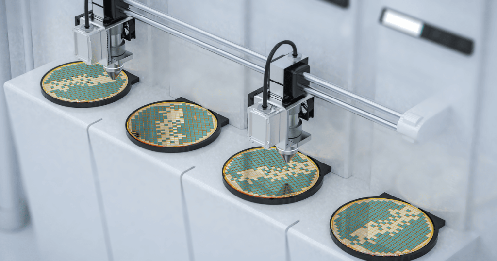
Artificial intelligence (AI) is rapidly transforming semiconductor inspection by enhancing the capabilities of imaging optics systems for automated defect detection and real-time quality control. By combining high-resolution optical imaging with machine learning and deep learning algorithms, manufacturers can achieve a new level of precision and efficiency in detecting, classifying, and responding to process anomalies.
Modern inspection systems leverage AI to analyze complex image datasets captured by high-resolution cameras and specialized optics. These systems can automatically identify and classify a wide range of defect types, including pattern irregularities, particle contamination, surface scratches, overlay errors, and more — tasks that traditionally required extensive manual review or rule-based software prone to false positives. With AI, defect classification becomes context-aware, improving detection accuracy even in densely patterned or noisy environments.
One of the key strengths of AI-enabled imaging systems lies in their ability to learn from historical inspection data. By training neural networks on labeled datasets from previous production runs, the system can not only recognize known defect types but also predict emerging failure modes based on subtle patterns or deviations that may not be apparent to human operators or conventional inspection tools. This predictive capability is invaluable for preventive maintenance, process optimization, and yield improvement.
AI also enables real-time decision-making, which is critical for inline inspection and control. Imaging data can be processed on-the-fly, allowing the system to provide immediate feedback to the production line. When defects are detected, the system can flag wafers for rework or adjust process parameters automatically, reducing downtime and minimizing waste.
In terms of hardware, AI integration often requires enhancements to the imaging optics system itself. This includes the use of multi-modal imaging (e.g., combining bright-field, dark-field, and infrared views), adaptive optics to adjust focus or illumination dynamically, and high-throughput image acquisition technologies to handle large volumes of data efficiently. Edge computing and GPU acceleration are also increasingly deployed to support the fast processing demands of AI inference engines.
3.3 Quantum Imaging and Sensing for Semiconductor Metrology
Quantum optics, especially through emerging fields like quantum imaging and quantum sensing, represents a groundbreaking frontier in semiconductor metrology. These techniques leverage fundamental quantum phenomena — such as entanglement, superposition, and squeezed light — to overcome classical limits in optical measurement, enabling unprecedented resolution, sensitivity, and signal-to-noise performance.
In conventional imaging systems, resolution is typically constrained by the diffraction limit, while sensitivity is limited by shot noise and environmental interference. Quantum imaging seeks to break through these barriers by using entangled photon pairs or quantum-correlated light sources, which allow for the acquisition of spatial or spectral information beyond classical limits. For example, quantum ghost imaging and quantum illumination can extract detailed structural information from a sample with fewer photons and greater resilience to noise — a major advantage in scenarios where fragile or low-reflectivity structures must be measured.
In the context of semiconductor manufacturing, quantum-based imaging systems are being explored for applications such as:
- Wafer inspection and defect detection at the atomic or molecular level, especially in densely packed circuits or buried layers.
- Critical dimension (CD) metrology, where quantum-enhanced interferometry could offer picometer-scale precision in measuring feature sizes and edge placement.
- Material characterization, including detection of impurities, dopant distributions, or stress/strain mapping using quantum sensors like nitrogen-vacancy (NV) centers in diamond.
Quantum sensing, often implemented through quantum-enhanced interferometry or magnetometry, enables measurements of minute changes in displacement, magnetic fields, or refractive index — with sensitivities far beyond classical sensors. For instance, squeezed light sources can reduce quantum noise in interferometric measurements, improving the detection of nanoscale variations in thin film thickness or lithographic alignment.
These quantum-enhanced systems also show promise for non-destructive evaluation (NDE), where low-intensity, high-sensitivity measurements are crucial. Moreover, as feature sizes in advanced semiconductor devices approach a few nanometers or even sub-nanometer scales, traditional inspection tools may no longer suffice. Quantum techniques offer a potential solution to bridge this gap by enabling imaging and measurement capabilities compatible with the demands of next-generation node development, including 2 nm and beyond.
4. Conclusion

Laser and imaging optics are playing an increasingly pivotal role in shaping the future of semiconductor technology, driving progress across the full spectrum of fabrication, from ultra-precise material processing to advanced metrology and defect inspection. These optical systems are not just supportive tools; they are foundational enablers of innovation, providing the accuracy, resolution, and versatility required to meet the ever-tightening tolerances of modern semiconductor devices.
As the industry pushes toward smaller nodes, 3D architectures, and heterogeneous integration, the performance demands placed on optical technologies have grown exponentially. Lasers are now used in a wide range of applications, including micromachining, dicing, laser annealing, patterning, and welding — often with femtosecond or picosecond precision to avoid thermal damage and maintain feature integrity. These laser processes rely on advanced beam delivery systems, high-stability optics, and real-time feedback mechanisms to achieve nanometer-level control.
In parallel, high-resolution imaging optics are essential for tasks such as wafer inspection, overlay alignment, critical dimension (CD) measurement, and defect analysis. With the integration of AI, adaptive optics, and multi-wavelength illumination strategies, these systems are evolving into intelligent platforms capable of not only identifying defects but also learning from them to enhance yield and process efficiency.
Furthermore, the convergence of optics and photonics in semiconductor platforms is opening up new frontiers, particularly in integrated photonic circuits, where light is used for on-chip communication, sensing, and computation. Optical systems are critical for both the manufacture and characterization of these devices, from waveguide alignment to mode field analysis.
With ongoing advancements in laser technology, quantum-enhanced imaging, EUV optics, and machine learning integration, the outlook for laser and imaging optics in semiconductor fabrication is both promising and transformative. These technologies will continue to play a central role in enabling faster, smaller, more efficient, and more powerful semiconductor devices, keeping pace with — and often driving — the demands of next-generation electronics.
5. Where to Purchase Quality Semiconductor Optics?

Wavelength Opto-Electronic designs and manufactures a broad range of semiconductor optics, from laser components, optical systems, imaging optics, to DIC microscopes for semiconductor applications. Utilizing cutting-edge technologies and manufacturing techniques, we’re also able to customize optics for your semiconductor requirements.
