
What is Microscopy? A Technical Microscopy Guide
Author: Bryan Ng – Marketing Manager
Published on:
Last edited:
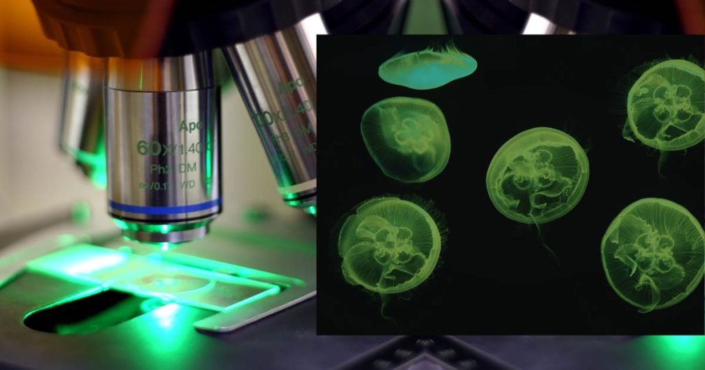
1. What is Microscopy?
Microscopy is the science and practice of using microscopes to observe objects and structures too small to be seen with the naked eye. From the earliest rudimentary magnifying lenses crafted in 17th-century Europe to today’s cutting-edge super-resolution and electron microscopy systems, microscopy has stood as a cornerstone of scientific discovery — enabling transformative breakthroughs in biology, medicine, materials science, semiconductor manufacturing, forensic analysis, and beyond.
The human eye can resolve features no smaller than approximately 100 micrometres (µm). Microscopy extends this capability by orders of magnitude, enabling scientists and engineers to observe individual cells, subcellular organelles, crystal lattice structures, nanoscale surface defects, and even single molecules. In doing so, it has redefined the boundaries of what is knowable in science and what is achievable in industry.
At its core, however, microscopy is about resolving detail — capturing fine spatial information with clarity, accuracy, and reproducibility. And the quality of that detail depends, above all else, on the optical components at the heart of the system, particularly the objective lens.
2. How a Microscope Works?
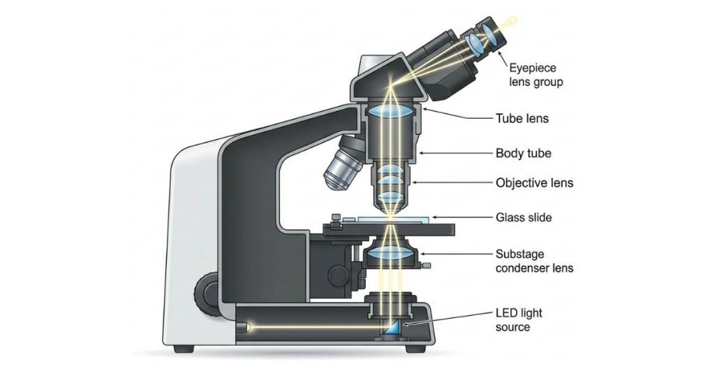
A modern compound microscope operates on the principle of multi-stage magnification through a series of precisely engineered optical elements. Light from an illumination source — or emitted by the specimen itself in the case of fluorescence — passes through the objective lens, which captures and focuses it to produce a magnified real image. This image is then either viewed through an eyepiece for direct observation or relayed to a digital camera sensor via a tube lens for capture, analysis, and archiving.
2.1 The Objective Lens
The primary optical element is positioned closest to the specimen. It determines the system’s resolution, magnification, depth of field, and light collection efficiency. It is, without question, the most critical component in the entire microscope.
2.2 The Tube Lens
The tube lens works in partnership with an infinity-corrected objective to converge the collimated rays emerging from the objective into a focused intermediate image. It plays a vital role in minimising optical aberrations and ensuring that the image projected onto the sensor or eyepiece is sharp and geometrically accurate.
2.3 The Eyepiece or Camera Sensor
The eyepiece or camera sensor delivers the final image to the observer or detector. In research and industrial settings, digital cameras are almost universally used, enabling image processing, quantitative analysis, and data archiving.
2.4 The Illumination System
Whether transmitted, reflected, laser, or LED-based — must be carefully matched to the objective’s spectral sensitivity and the imaging modality in use.
Understanding the physics and engineering behind each of these components is essential to selecting the right microscopy configuration for a given application, and to interpreting the images it produces with confidence.
3. Key Optical Parameters in Microscopy
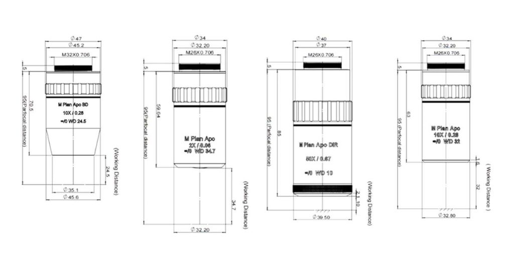
To make informed decisions about microscopy systems and components, practitioners must understand the fundamental optical parameters that govern performance.
3.1 Numerical Aperture
Numerical Aperture (NA) is arguably the single most important specification in microscopy. It is a dimensionless number that quantifies the range of angles over which the objective can accept or emit light, and it directly governs both resolution and light-gathering power. The theoretical resolution limit of an objective is given by the Rayleigh criterion: Resolution (µm) = 0.61 × λ / NA, where λ is the wavelength of light used. A higher NA enables finer features to be resolved. For instance, an objective with NA = 0.90 operating at 550 nm visible light can theoretically resolve features as small as approximately 0.37 µm. In practical terms, the NA also determines how efficiently the system collects fluorescence signal or scattered light — a critical consideration in low-light imaging applications.
3.2 Working Distance
Working Distance (WD) is the physical gap between the front lens element of the objective and the focal plane of the specimen when the specimen is in sharp focus. This parameter is of immense practical importance. High-magnification objectives with high NA tend to have very short working distances — sometimes less than 1 mm — which limits access to the specimen and constrains the design of sample holders. In contrast, long working distance (LWD) objectives sacrifice some NA in exchange for greater clearance, enabling imaging through thick substrates, environmental chambers, or industrial enclosures.
3.3 Depth of Field
Depth of Field (DOF) defines the axial range over which the specimen remains acceptably in focus. It is inversely proportional to the square of the NA — meaning that as NA increases, depth of field decreases rapidly. For a high-NA objective at NA = 0.90, the depth of field may be only a fraction of a micrometre. This demands extremely precise axial positioning of the sample, typically achieved via motorised z-stages with sub-micrometre resolution.
3.4 Field of View (FOV)
Field of View (FOV) determines the lateral extent of the specimen that can be imaged in a single frame. At low magnification (e.g. 1X), an objective may cover an entire 24 mm field. At 100X, this narrows to less than 0.25 mm. Balancing FOV against resolution is a fundamental design trade-off in microscopy: high magnification delivers fine detail within a small area, while low magnification surveys a larger area at reduced resolution. In many workflows, a combination of magnifications is used — low magnification for overview scanning, high magnification for detailed inspection.
3.5 Chromatic and Spherical Aberration
Chromatic aberration causes different wavelengths of light to come to focus at different axial positions, producing colour fringing and blurring in broadband imaging. Spherical aberration arises when rays passing through different radial zones of the lens come to focus at different points. Objective lens design is largely an exercise in correcting these aberrations across the relevant spectral range — a task that defines the difference between achromatic, semi-apochromatic, and fully apochromatic objectives.
4. Types of Microscopy
Microscopy is not a single technique but a broad family of methods, each tailored to particular specimen types, contrast mechanisms, and information requirements.
4.1 Bright-Field Microscopy
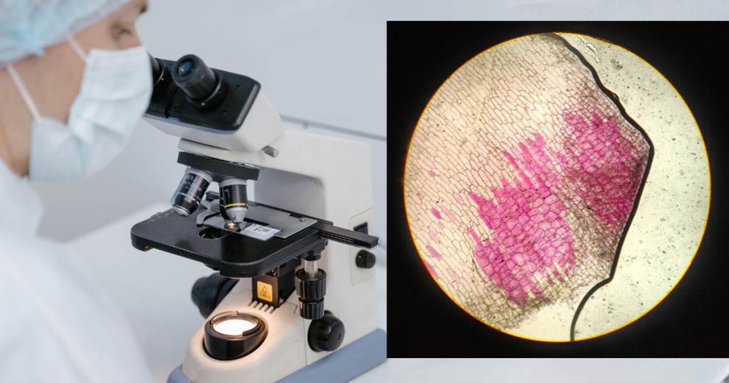
This is the most widely used and historically oldest form of optical microscopy. The specimen is illuminated by transmitted or reflected white light, and contrast arises from the specimen’s absorption, scattering, or reflection of that light. It is well-suited for stained biological tissue sections, opaque industrial materials, and routine quality control inspection.
4.2 Fluorescence Microscopy
Fluorescence microscopy specimens are labelled with fluorescent dyes or genetically encoded fluorescent proteins, which are excited by a specific wavelength of light and emit at a longer wavelength. By using appropriate excitation and emission filters, multiple fluorescent labels can be imaged simultaneously, revealing the spatial organisation of proteins, nucleic acids, lipids, and organelles with extraordinary specificity. Objective lenses used here must exhibit minimal autofluorescence and high transmission across UV-to-NIR wavelengths.
4.3 Confocal Microscopy
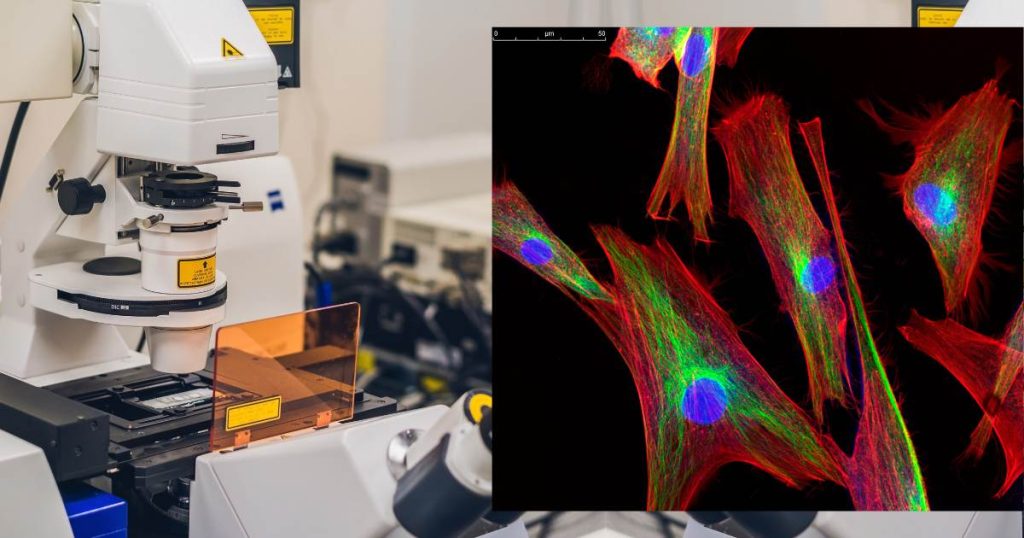
A pinhole aperture conjugate to the focal plane physically blocks out-of-focus fluorescence from reaching the detector, enabling optical sectioning — acquiring sharp, high-contrast images at defined depths within a three-dimensional specimen. By collecting a stack of optical sections at different z-positions, a complete 3D reconstruction can be assembled. Confocal microscopy is extensively used in neuroscience, developmental biology, cancer research, and semiconductor materials analysis.
4.4 Differential Interference Contrast (DIC) Microscopy
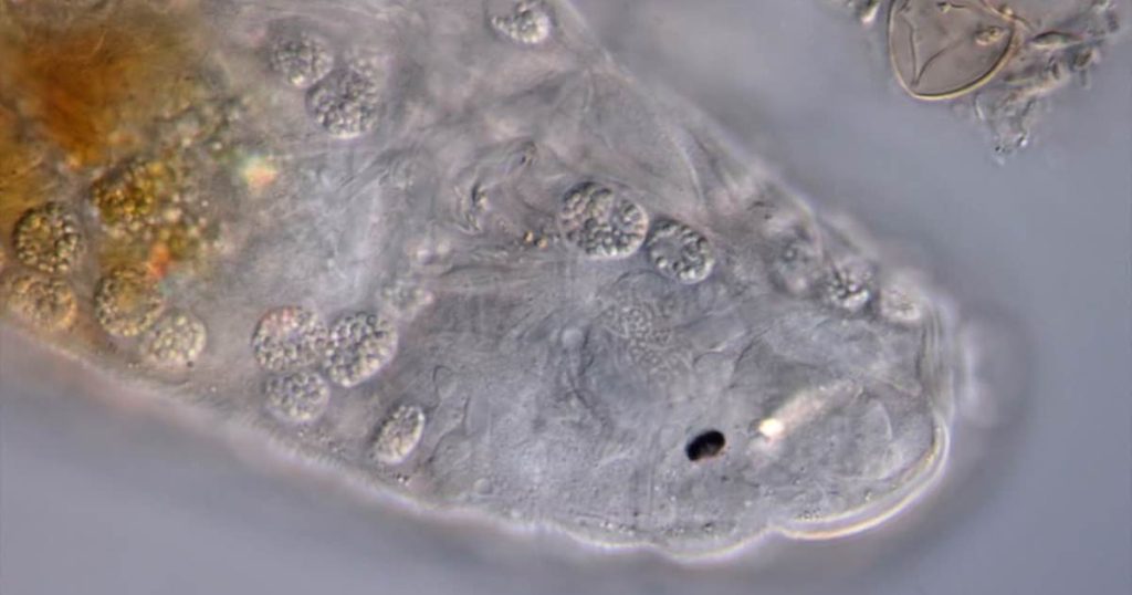
DIC uses polarised light and a Nomarski prism to produce pseudo-three-dimensional images of transparent, unstained specimens — such as living cells, embryos, or optically smooth surfaces — revealing surface topology and internal refractive index variations with exceptional sensitivity. It is particularly valuable for live-cell imaging where fluorescent labelling is undesirable or impractical.
4.5 Near-Infrared (NIR) Microscopy
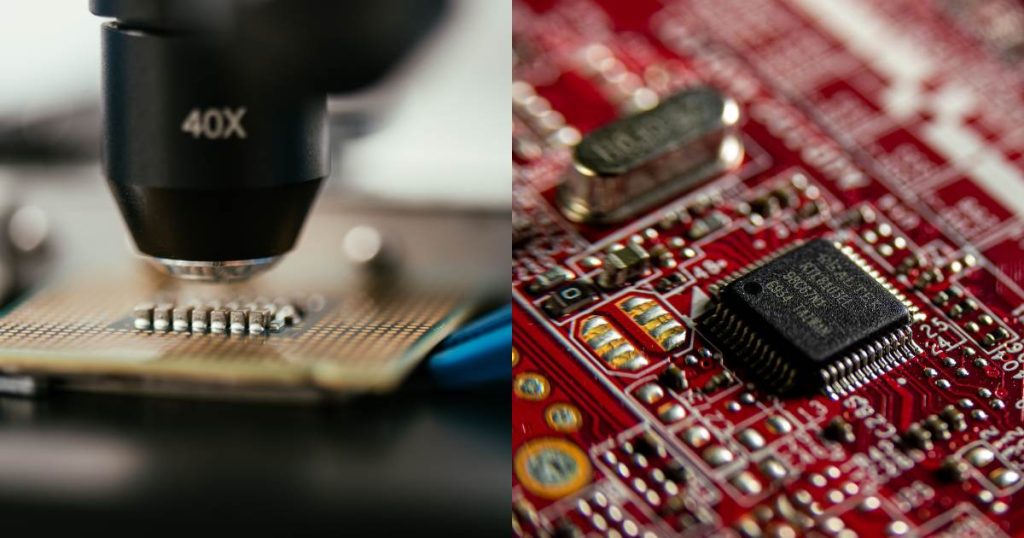
It operates at wavelengths between approximately 700 nm and 1,100 nm. Silicon, which is opaque at visible wavelengths, becomes transparent in this range — making NIR microscopy indispensable for backside inspection of silicon semiconductor devices. NIR microscopy is also used for deep-tissue imaging in biomedical applications, where longer wavelengths scatter less and enable greater imaging depth.
4.6 Near-Ultraviolet (NUV) Microscopy
Operating at wavelengths from 355 nm to 405 nm, NUV microscopy enables higher spatial resolution than visible-light systems and is widely used in photomask inspection, UV laser microfabrication process monitoring, and semiconductor lithography.
4.7 Super-Resolution Microscopy
Encompassing techniques such as STED, STORM, and PALM, super-resolution microscopy circumvents the classical diffraction limit to achieve spatial resolutions of tens of nanometres. These methods place extremely demanding requirements on objective lens quality, particularly in terms of NA, aberration correction, and transmission efficiency.
5. The Role of the Objective Lens
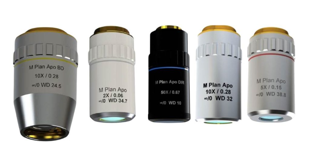
The objective lens is the optical heart of any microscope — where light interacts most critically with the specimen and where the fundamental limits of resolution and contrast are set. Choosing the wrong objective results in blurred images, poor signal-to-noise ratios, chromatic artefacts, and lost information.
5.1 Apochromatic Correctio
Apochromatic (APO) objectives are corrected at three or more wavelengths, delivering flat, sharp, colour-accurate images across the full spectral range of interest. This is essential for multi-channel fluorescence imaging, where simultaneous or sequential acquisition at multiple wavelength bands must produce co-registered images free of chromatic offset.
5.2 Infinity-Corrected Optical Design
In an infinity-corrected system, the objective produces a collimated beam between itself and the tube lens. This intermediate collimated space allows beamsplitters, filters, waveplates, and other optical components to be inserted without disturbing the focus — an essential requirement for complex configurations such as fluorescence filter cubes, laser delivery systems, and polarisation optics.
6. Wavelength Opto-Electronic Microscope Objective Lenses
For researchers, engineers, and system integrators who demand precision at every level, Wavelength Opto-Electronic offers an extensive range of over 40 microscope objective lenses engineered for the most rigorous scientific and industrial applications. Each lens in the portfolio is designed as an infinity-corrected apochromatic system, available across visible, NIR, and NUV spectral ranges.
6.1 M-PlanAPO Series — Apochromatic Infinity-Corrected Objectives
Delivers apochromatic correction across the 400–700 nm visible spectrum in magnifications from 1X to 50X, with numerical apertures spanning 0.025 to 0.550. Ideal for real-time coaxial laser processing monitoring, micro-imaging, DIC imaging, fluorescence inspection in biomedical research, and precision laser repair of touch panels and solar cells.
6.2 M-PlanAPO-HR Series — High Resolution Objectives
Pushes performance further with NA values reaching 0.900 at 100X magnification and a resolution capability of just 0.30 µm. The choice for applications where maximum spatial detail is non-negotiable — including advanced semiconductor inspection, nanoscale surface metrology, and high-content fluorescence screening.
6.3 M-PlanAPO-SL Series — Super Long Working Distance Objectives
Addresses applications where physical clearance between the objective and specimen is critical. With working distances up to 30 mm at 20X, the SL series enables imaging through environmental chambers, heated stages, microfluidic devices, or custom industrial enclosures without compromising optical quality.
6.4 NIR Objective Series — Infrared Optimised
Optimised for 532 nm and 1030–1064 nm wavelengths, purpose-built for silicon wafer backside inspection, NIR fluorescence imaging, and femtosecond laser microfabrication. The M-PlanAPO-HRNIR-50X achieves an impressive NA of 0.750 with a 4 mm working distance, offering exceptional resolution for NIR laser processing applications.
6.5 NUV Objective Series — Ultraviolet Optimised
Supports 355 nm, 365 nm, 405 nm, and 532 nm wavelengths for UV photomask inspection, UV laser microfabrication, and semiconductor lithography monitoring. The M-PlanAPO-HRNUV-50X delivers NA 0.650 with 10 mm working distance — combining high resolution with practical working clearance.
6.6 LCD-PlanAPO Series — Cover Glass Corrected
Provides NIR and NUV objectives with integrated cover glass correction options (t0, t0.7, and t1.1 mm), ensuring diffraction-limited performance when imaging through standard microscope coverslips — essential in life science applications where samples are routinely mounted beneath glass coverslips.
6.7 PlanFluor-EPI Series — Fluorescence Optimised Eyepiece Objectives
Specifically optimised for epi-illumination fluorescence microscopy, offering NA values up to 0.90 at 100X with a 25 mm field number. Available in both W4/5″ and M26 x 0.706 thread formats for compatibility with a wide range of upright and inverted fluorescence microscope platforms.
6.8 TL-200-70 Tube Lens
Designed for use with any of the above infinity-corrected objectives, the TL-200-70 (EFL: 200 mm, WD: 60.36 mm) focuses the collimated output beam into a sharp, well-corrected intermediate image with minimal aberration, completing the optical system.
Customisation is available across the entire range for OEM customers and research institutions requiring bespoke specifications — including modified working distances, specialised coatings, alternative thread formats, or entirely custom optical designs. Contact us to discuss your requirements.
7. Choosing the Right Objective Lens
Selecting the optimal objective requires carefully matching several parameters to your specific application and system design.
7.1 Wavelength Range
Determine whether your application operates in the visible, NIR, or NUV spectrum and select an objective whose glass and coatings are optimised for that range.
7.2 Magnification and NA
Higher magnification and NA deliver finer resolution but reduce FOV and working distance. Define your resolution requirement first, then select the lowest magnification that meets it.
7.3 Working Distance
Assess the geometry of your sample and sample holder. Enclosed chambers, thick substrates, or industrial setups typically require long working distance variants.
7.4 Cover Glass Correction
If imaging through a coverslip, use an LCD-series corrected objective matched to your coverslip thickness to avoid spherical aberration-induced image degradation.
7.5 Application Environment
Consider whether the objective will be used in a clean laboratory, industrial production line, or laser processing workstation, as this affects the required mechanical robustness and contamination resistance.
8. Applications of Precision Microscopy
8.1 Biomedical and Life Sciences
High-NA apochromatic objectives are the standard tool for cell biology, pathology, genomics, and pharmaceutical drug discovery. Multi-channel fluorescence and confocal imaging with the M-PlanAPO and PlanFluor-EPI series supports the most demanding biological imaging workflows.
8.2 Semiconductor and Wafer Inspection
NIR objectives enable backside inspection of silicon devices at 1064 nm, where silicon is transparent — revealing buried interconnects, voids, and defects invisible to visible-light systems. The M-PlanAPO-NIR and HRNIR series are purpose-built for this application.
8.3 Laser Microfabrication and Processing
Precision laser cutting, drilling, welding, and surface structuring at micron scales require objectives with tight beam focus, long working distances, and high laser damage thresholds. The M-PlanAPO-SL and NIR series are optimised for coaxial laser delivery and real-time process monitoring.
8.4 Legal and Historical Document Analysis
Long working distance objectives with visible and NIR capabilities allow non-contact imaging of fragile historical documents, artworks, and forensic evidence — revealing hidden text, ink composition, and forgery traces without physical contact or risk of damage.
8.5 Medical Optical Imaging
From endoscopy to ophthalmology and surgical guidance, precision objective lenses enable high-resolution in-vivo imaging across a range of medical modalities. Wavelength Opto-Electronic’s objective range supports the optical requirements of diverse medical imaging system architectures.
9. Conclusion
Microscopy is far more than magnification. It is the science of seeing clearly — with precision, at scale, and across a spectrum of wavelengths — and translating what is seen into knowledge and capability. Every advance in microscopy has opened new windows onto the physical world, from the discovery of the cell to the imaging of individual atoms, from the inspection of nanoscale transistors to the visualisation of live neural activity.
It remains the defining optical element in this endeavour. Its numerical aperture sets the resolution ceiling. Its spectral correction determines chromatic fidelity. Its working distance defines what specimens and configurations are accessible. And its aberration correction separates publishable data from artefact-riddled noise.
Whether you are building a fluorescence imaging platform for life sciences, an NIR inspection system for semiconductor quality control, or a UV laser processing workstation for precision manufacturing, the objective lens is where performance is won or lost. Wavelength Opto-Electronic’s range of over 40 microscope objective lenses — spanning visible, NIR, and NUV spectral bands, in standard, high-resolution, long working distance, and cover glass corrected variants — provides the optical foundation for the most demanding microscopy applications in research and industry.
