
SWIR Semiconductor Inspection: How the Right SWIR Lens Makes All the Difference
Author: Bryan Ng – Marketing Manager
Published on:
Last edited:
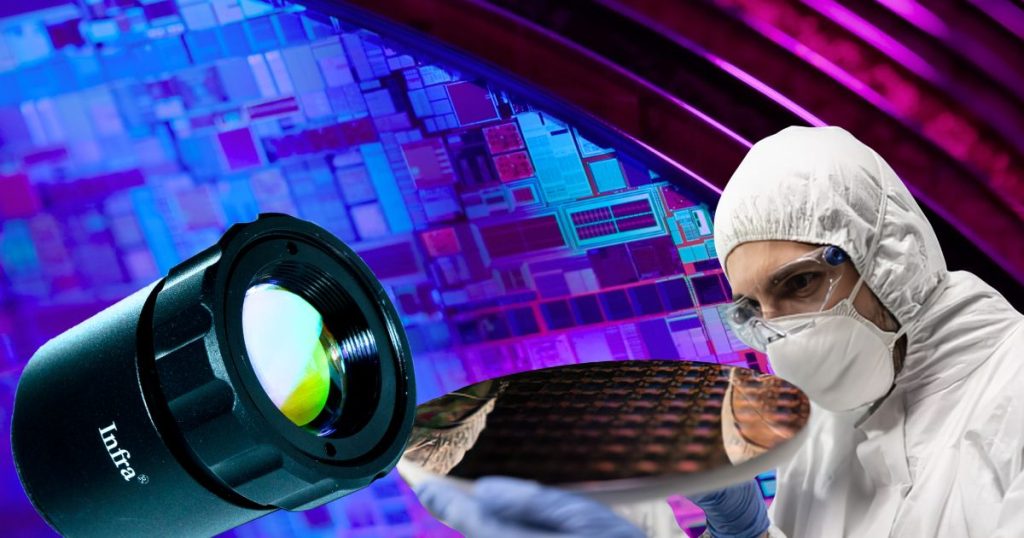
Semiconductor manufacturing leaves no room for error. A single undetected subsurface crack, a void buried beneath a flip chip, or a delamination hidden inside a die attach layer can lead to device failure in the field — with consequences ranging from product recalls to safety incidents in automotive or industrial applications. As chip architectures grow more complex and package geometries shrink, traditional optical inspection methods are no longer sufficient.
Short-wave infrared (SWIR) imaging has become a critical, non-destructive inspection technology in modern semiconductor fabs and packaging lines. It enables engineers and quality teams to see through silicon itself — revealing defects that are completely invisible to visible-light cameras and conventional AOI systems. But the quality of a SWIR inspection system depends heavily on one often-overlooked component: the lens.
This guide explains how SWIR semiconductor inspection works, what it can detect, and why selecting a purpose-built SWIR lens — such as those in Wavelength Opto-Electronic’s Infra® SWIR lens series — is fundamental to achieving reliable, high-resolution inspection results.
1. What Is SWIR Imaging and Why Does It Matter for Semiconductors?
SWIR refers to light in the short-wave infrared spectrum, generally defined as wavelengths between 0.9 µm and 1.7 µm (with extended SWIR reaching to 2.5 µm). This range sits just beyond the visible and near-infrared (NIR) regions, and it interacts with materials in fundamentally different ways from visible light.
SWIR cameras — most commonly built around indium gallium arsenide (InGaAs) sensors — detect reflected or transmitted SWIR light. Unlike thermal infrared cameras that image emitted heat, SWIR imaging is a reflectance and transmission technique. This makes it highly sensitive to structural features and material interfaces within a sample.
The property that makes SWIR uniquely powerful for semiconductor inspection is silicon’s optical transparency in this band. Silicon has a bandgap energy of approximately 1.12 eV, corresponding to a wavelength of around 1100 nm. At wavelengths longer than this threshold, photons do not have enough energy to be absorbed by the silicon lattice — they pass straight through. This means a SWIR imaging system can look directly through a silicon wafer or die and image the structures beneath the surface, without any cutting, polishing, or chemical decapsulation.
This is the foundation of transillumination SWIR inspection: placing a SWIR light source on one side of the sample and an InGaAs camera equipped with a SWIR lens on the other. Any structural disruption — a crack, void, delamination, or inclusion — appears as a contrast feature in the transmitted image.
2. Key Applications of SWIR in Semiconductor Inspection
2.1 Wafer-Level Defect Detection

During wafer fabrication and dicing, micro-cracks are routinely introduced into the silicon — along dicing streets, at grinding-induced subsurface damage zones, or at epitaxial layer interfaces. Many of these defects are buried below the surface and completely invisible under visible-light microscopy.
SWIR transillumination imaging can detect all of these with high spatial resolution. In production environments, a SWIR area or line-scan camera combined with appropriate SWIR optics can perform full-wafer inspection at throughputs compatible with automated wafer handling. Subsurface crack networks are flagged before they propagate further during downstream thermal cycling or wire bonding operations.
For thin wafers — increasingly common in power devices, RF components, and 3D IC integration — this is especially critical. Handling-induced micro-cracks in 100 µm or thinner wafers can be catastrophic. Early SWIR detection allows fabs to remove compromised wafers before they cost more in downstream yield loss.
2.2 Die Attach and Flip Chip Void Inspection
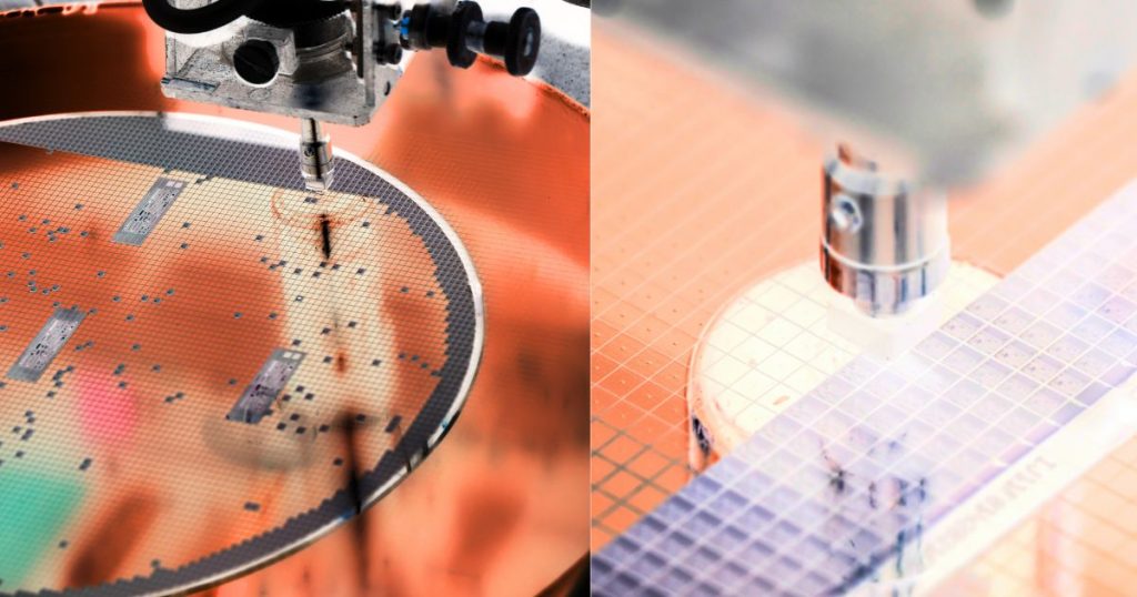
Die attach void inspection is one of the highest-value applications of SWIR imaging in back-end semiconductor packaging. When a silicon die is mounted to a substrate or leadframe using adhesive, solder paste, or sintered silver, voids can form in the bond layer. These voids degrade thermal conductivity, concentrate mechanical stress, and trap moisture — contributing to premature device failure under thermal cycling.
In flip chip packages, the die is bonded face-down through solder bumps. The die itself acts as a natural SWIR window: the camera images through the back of the silicon die to inspect the solder bumps and underfill layer below. SWIR imaging can reveal voids in die attach materials, delamination at die-substrate interfaces, underfill voiding or incomplete fill, and cracked or collapsed solder bumps — all without touching the package.
This makes SWIR a compelling, cost-effective alternative to X-ray screening for silicon-based packages, and a significantly faster option than acoustic microscopy (C-SAM) for production-line void screening.
2.3 IC Package Inspection Through Encapsulant
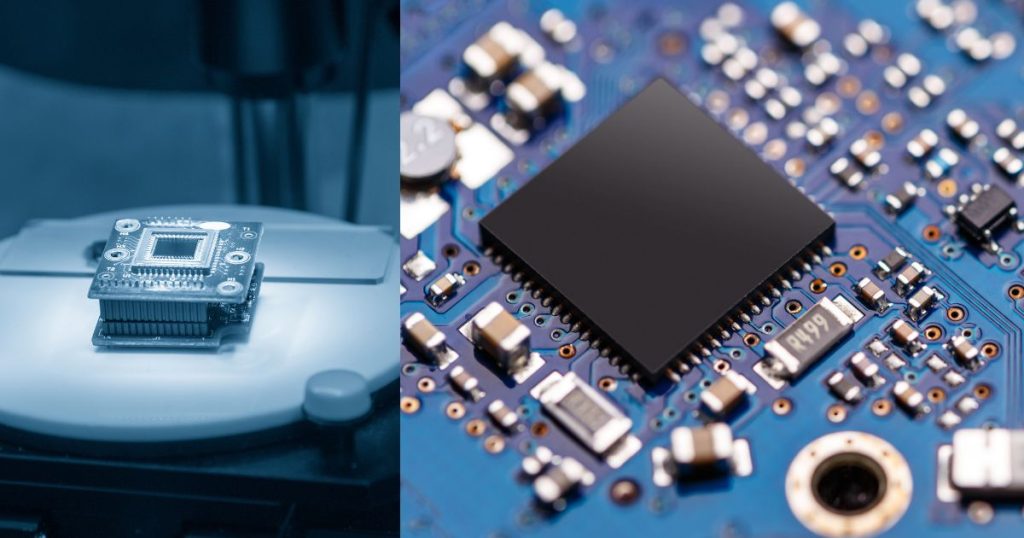
Many standard epoxy molding compounds (EMC) used to encapsulate semiconductor packages exhibit partial transparency at SWIR wavelengths. This allows SWIR cameras to image through the encapsulant and inspect bond wires, die position, and internal structural integrity — without any decapsulation.
Bond wire inspection through encapsulant is a standout application. Wire sweep (bond wire displacement during molding) and wire sag can cause shorts or opens that are difficult to detect non-destructively. SWIR imaging can detect wire position anomalies through many EMC materials, enabling 100% non-destructive inspection of encapsulated packages.
2.4 Power Device Inspection for Automotive Applications

Power semiconductors — IGBTs, MOSFETs, and diodes used in EV inverters, industrial drives, and power conversion — are packaged under particularly stringent reliability requirements. Die attach void levels directly affect thermal resistance (Rth), which governs the device’s power-handling capability and long-term reliability under thermal cycling.
Automotive manufacturers and Tier 1 suppliers follow AEC-Q101 qualification standards that specify maximum allowable void area percentages. SWIR imaging systems are increasingly integrated into inline production testers for 100% die attach void inspection of automotive power modules — replacing or complementing X-ray inspection with faster, radiation-free throughput.
2.5 Solar Cell and Photovoltaic Manufacturing

Silicon solar cells share the same SWIR transparency as semiconductor dies. In photovoltaic manufacturing, SWIR inspection is widely used to detect micro-cracks introduced during cell cutting, stringing, and module lamination, as well as metallization defects in the finger grid and busbar network.
Modern solar manufacturing lines run at very high throughput with large cell formats (M10/G12, up to 210 mm × 210 mm). SWIR line-scan inspection systems with high-resolution, high-throughput optics are essential for achieving the detection sensitivity needed to maintain yield at GW-scale production rates.
3. Why SWIR Lens Is the Most Critical Optical Component
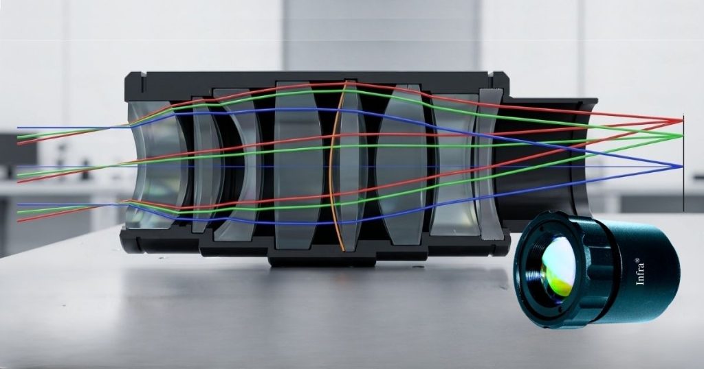
In any SWIR imaging system, the sensor (InGaAs detector) receives most of the attention. But the lens is equally critical — and a common source of underperformance in poorly specified systems.
Standard visible-light camera lenses are not suitable for SWIR inspection. They are designed with glass formulations, element configurations, and anti-reflection coatings optimized for the 400–700 nm visible band. At SWIR wavelengths:
- Chromatic aberration increases significantly — elements corrected for visible wavelengths shift focus unpredictably in the SWIR band
- Transmission drops — many optical glass types absorb heavily above 1000 nm
- Anti-reflection coatings become ineffective — coatings optimized for visible light reflect significant portions of SWIR energy, reducing contrast and throughput
The result is blurred images, reduced resolution, poor contrast, and inconsistent focus across the field — all of which directly impair defect detectability. In semiconductor inspection, where the target may be a 50 µm void or a hairline micro-crack, these compromises are unacceptable.
A purpose-built SWIR lens solves all of these issues through specialized glass selection, optical design, and coating technology.
4. Wavelength Opto-Electronic’s Infra® SWIR Lenses: Built for Semiconductor Inspection
Wavelength Opto-Electronic’s Infra® SWIR lens series is specifically engineered for demanding industrial and scientific SWIR imaging applications, including semiconductor inspection. The range covers wavelengths from 0.9 µm to 1.7 µm (core SWIR band) as well as 0.9 µm to 2.5 µm (extended SWIR) and 1.5 µm to 5.0 µm (MWIR/extended infrared), providing coverage across all relevant inspection wavelengths.
4.1 Broad Focal Length Range
The Infra® series spans focal lengths from 14 mm to 200 mm, enabling configurations from wide-field wafer-level inspection to high-magnification die and bump inspection:
- 14 mm (Infra-SW141.1-15) — wide-field imaging for large-area wafer or substrate inspection at close working distances
- 25 mm — versatile general-purpose focal length, available in multiple aperture and detector configurations
- 50 mm — standard inspection focal length balancing field of view and resolution
- 75 mm — mid-telephoto option for increased working distance in inline conveyor systems
- 100 mm — telephoto for detailed die or package inspection at greater standoff
- 200 mm — long focal length for specialized high-magnification or remote-sensing inspection setups
This range ensures engineers can match the lens to the specific inspection geometry — whether imaging a full 300 mm wafer from a fixed standoff or resolving individual solder bumps on a fine-pitch flip chip package.
4.2 InGaAs Detector Compatibility
Infra® SWIR lenses are matched to the most common InGaAs sensor formats used in industrial SWIR cameras:
- 640 × 480, 25 µm pixel pitch — widely used area scan format for general inspection
- 640 × 512, 15 µm pixel pitch — higher resolution for tighter feature detection
- 1280 × 1024, 10 µm pixel pitch — high-resolution format for fine-feature inspection (available in selected models such as the Infra-SW2003.0-21)
- 1024 × 768, 17 µm pixel pitch — mid-resolution format for extended SWIR bands
- 320 × 256, 30 µm pixel pitch — compact format for space-constrained or lower-cost configurations
Matching lens optical design to detector pixel pitch is essential: a lens with insufficient resolution for a 10 µm pixel sensor will waste the sensor’s resolving capability, while a lens overspecified for a 30 µm pixel sensor adds unnecessary cost and bulk. Wavelength Opto-Electronic’s product matrix makes it straightforward to identify the right lens-sensor pairing for a given application.
4.3 Fast Apertures for Low-Light SWIR Imaging
SWIR imaging of silicon in transmission mode requires sufficient photon flux to achieve good signal-to-noise at the detector. Infra® SWIR lenses offer fast apertures — including F/1.1 (Infra-SW141.1-15) and F/1.4 — that maximize light collection and enable shorter exposure times. This is particularly important for inline inspection systems where cycle time is constrained, or for imaging thicker silicon substrates where SWIR attenuation reduces transmitted intensity.
4.4 Mounting Flexibility
Infra® lenses are available with C-mount, M37×0.5, Bayonet, and proprietary 25.4-32TPI thread mounts, covering the standard interfaces used in industrial InGaAs cameras from all major manufacturers. This simplifies system integration and ensures mechanical compatibility across a range of camera platforms.
4.5 Customization Capability
Wavelength Opto-Electronic offers custom optical design and system customization for applications with requirements beyond the standard product range. This includes custom focal lengths, modified back working distances (BWD), non-standard mounts, specialized AR coatings for narrow-band SWIR illumination, and integration into larger optical assemblies. For OEM inspection system developers and fab equipment integrators, this makes Wavelength Opto-Electronic a single-source partner for both standard and application-specific SWIR optics.
5. Selecting the Right Infra® SWIR Lens for Semiconductor Inspection
Choosing the correct lens for a semiconductor SWIR inspection application involves several key parameters:
1. Wavelength range. For silicon wafer and die inspection (transillumination), the 0.9–1.7 µm range is optimal — this is where InGaAs sensitivity is highest, and silicon transmission is strong. For extended SWIR or MWIR applications (some encapsulant materials, certain compound semiconductors), the 1.5–5.0 µm Infra® lenses are appropriate.
2. Focal length and working distance. Determine the required field of view and available working distance in your inspection setup. Shorter focal lengths (14–25 mm) suit close-range, wide-field applications; longer focal lengths (75–200 mm) are appropriate when the lens must be placed further from the sample — common in inline conveyor systems or when the inspection chamber has physical constraints.
3. Detector format. Match the lens image circle and resolution specification to your InGaAs camera’s sensor size and pixel pitch. Using a lens designed for a 640×480/25 µm sensor on a 1280×1024/10 µm sensor will result in corner softness and underutilized resolution.
4. Aperture. Faster F/# (lower number) collects more light — beneficial for thick silicon, low-illumination setups, or fast frame rates. If depth of field is the priority (e.g., for inspecting warped substrates), a slightly slower aperture may be preferable for the extended focal range it provides.
5. Mount compatibility. Verify C-mount or bayonet compatibility with the target InGaAs camera. For custom or OEM builds, Wavelength Opto-Electronic can accommodate non-standard mount interfaces.
6. Integrating Infra® SWIR Lenses Into Your Inspection System
Wavelength Opto-Electronic supports the full inspection system integration process, not just lens supply. Their product portfolio includes complementary components that work alongside Infra® SWIR lenses in a complete inspection system:
- Area scan and line scan cameras — compatible SWIR-capable camera platforms for both area and high-speed line-scan inspection
- Machine vision lighting — SWIR-compatible illumination sources for transillumination and reflectance inspection setups
- Bandpass filters — narrow-band optical filters to improve contrast by selecting specific SWIR wavelengths matched to the illumination source
- Telecentric lenses — for applications requiring accurate dimensional measurement of void area or crack dimensions free of parallax distortion
- Optical design and system customization services — for integrators building custom inspection platforms
This ecosystem approach means that engineers specifying a new SWIR semiconductor inspection station can source optically matched, application-validated components from a single supplier rather than assembling components from multiple vendors with uncertain compatibility.
7. SWIR Semiconductor Inspection: Choosing a Technology Partner
For semiconductor engineers and equipment buyers evaluating SWIR inspection, the lens selection is not a commodity decision. The wrong lens — whether a repurposed visible-band lens or an infrared lens with the wrong wavelength coverage or insufficient resolution — will limit the sensitivity of the entire inspection system, regardless of how capable the InGaAs camera is.
Wavelength Opto-Electronic has built the Infra® SWIR lens series with the rigorous requirements of industrial semiconductor inspection in mind: broad wavelength coverage, a complete focal length range matched to standard InGaAs detector formats, fast apertures for transmission imaging through silicon, and custom design capability for demanding OEM applications.
As semiconductor packages continue to advance — toward thinner silicon, finer bump pitches, more complex die-attach structures, and higher automotive reliability requirements — the need for high-performance, purpose-built SWIR optics will only grow. Partnering with an optics supplier that understands both the imaging physics and the manufacturing constraints of SWIR semiconductor inspection is the right foundation for building inspection capability that scales with the technology.
8. Conclusion
SWIR semiconductor inspection leverages silicon’s natural transparency to short-wave infrared light to reveal subsurface defects — cracks, voids, delaminations, and bond wire anomalies — that are invisible to every other non-destructive method. It is fast, radiation-free, and compatible with inline production environments, making it the inspection technology of choice for wafer inspection, die attach quality control, flip chip void detection, and automotive power device qualification.
The performance of any SWIR inspection system is only as good as its optics. Wavelength Opto-Electronic’s Infra® SWIR lens series provides semiconductor engineers and system integrators with a comprehensive, purpose-built lens portfolio — covering 0.9 µm to 5.0 µm, focal lengths from 14 mm to 200 mm, and detector formats from 320×256 to 1280×1024 — backed by custom optical design capability and a full ecosystem of complementary SWIR imaging components.
| Part Number | Wavelength (µm) | Focal Length (mm) | Focus Type | F# | BWD (mm) | Mount | Detector |
|---|---|---|---|---|---|---|---|
| LSW02514640 *NEW* | 0.9 – 1.7 | 25 | Manual | 1.4 | 4.3 | 25.4-32TPI | 640 x 480, 25µm |
| LSW02520640 *NEW* | 0.9 – 1.7 | 25 | Manual | 2.0 | 9.9 | C-Mount | 640 x 480, 25µm |
| Infra-SW141.1-15 *NEW* | 0.9 – 1.7 | 14 | Manual | 1.1 | 9.4 | C-Mount | 640 x 512, 15µm |
| LSW20024640V2 | 0.9 – 1.7 | 200 | Manual | 2.4 | 13.5 | C-Mount | 640 x 512, 15µm |
| LSW07515640 | 0.9 – 1.7 | 75 | Manual | 1.5 | 12.5 | C-Mount | 640 x 480, 25µm |
| LSW05014640 | 0.9 – 1.7 | 50 | Manual | 1.4 | 6.7 | M37x0.5 | 640 x 480, 25µm |
| Infra-SW2003.0-21 | 0.9 – 1.7 | 200 | Manual | 3.0 | 12.5 | C-Mount | 1280 x 1024, 10µm |
| Infra-SW122.5-15 | 1.5 – 5.0 | 12 | Manual | 2.5 | 33.1 | Bayonet | 640 x 512, 15µm |
| Infra-SW252.5-15 | 1.5 – 5.0 | 25 | Manual | 2.5 | 33.1 | Bayonet | 640 x 512, 15µm |
| Infra-SW253.0-17 | 1.5 – 5.0 | 25 | Manual | 3.0 | 33.1 | Bayonet | 1024 x 768, 17µm |
| Infra-SW502.5-15 | 1.5 – 5.0 | 50 | Manual | 2.5 | 33.1 | Bayonet | 640 x 512, 15µm |
| Infra-SW502.3-17 | 1.5 – 5.0 | 50 | Manual | 2.3 | 39.4 | Bayonet | 1024 x 768, 17µm |
| Infra-SW1002.3-17 | 1.5 – 5.0 | 100 | Manual | 2.3 | 33.1 | Bayonet | 1024 x 768, 17µm |
| Infra-SW1002.5-15 | 1.5 – 5.0 | 100 | Manual | 2.5 | 33.1 | Bayonet | 640 x 512, 15µm |
| Infra-SW2002.5-15 | 1.5 – 5.0 | 200 | Manual | 2.5 | 33.1 | Bayonet | 640 x 512, 15µm |
| Infra-SW252.5-30 | 0.9 – 2.5 | 25 | Manual | 2.5 | 13.5 | C-mount | 320 x 256, 30µm |
| Infra-SW352.0-30 | 0.9 – 2.5 | 35 | Manual | 2.0 | 13.4 | C-mount | 320 x 256, 30µm |
| Infra-SW502.0-30 | 0.9 – 2.5 | 50 | Manual | 2.0 | 13.5 | C-mount | 320 x 256, 30µm |
| Infra-SW752.0-30 | 0.9 – 2.5 | 75 | Manual | 2.0 | 13.5 | C-mount | 320 x 256, 30µm |
| Infra-SW1002.0-30 | 0.9 – 2.5 | 100 | Manual | 2.0 | 13.5 | C-mount | 320 x 256, 30µm |
| Infra-SW2002.0-30 | 0.9 – 2.5 | 200 | Manual | 2.0 | 13.5 | C-mount | 320 x 256, 30µm |
