
Precision Optical Systems for TGV Manufacturing with fs Laser
Application Note Serial No.: AN-SGYL-01-03-26
Author: Dr. Qu Yingli – R&D Director
Editor: Bryan Ng – Marketing Manager
Published on:
Last edited:
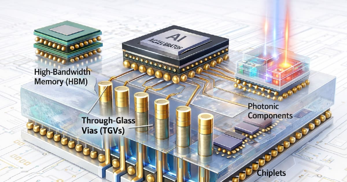
Through Glass Vias (TGV) are a critical enabling technology for advanced electronic and photonic packaging, with expanding applications in RF and mmWave modules, high-density interposers, MEMS packaging, image sensors, and integrated photonics. They enable reliable vertical electrical interconnections through glass substrates, supporting compact three-dimensional architectures and heterogeneous integration across multiple device platforms.
In emerging AI-driven systems such as AI accelerators, high bandwidth memory (HBM) integration, chiplet-based architectures, and advanced co-packaged optics, TGVs play an increasingly important role by providing low-loss, high-density vertical interconnections with excellent thermal and dimensional stability. Their material properties help maintain precise alignment and structural integrity, which are essential for tightly integrated multi-chip systems operating at high data rates.
Compared with conventional silicon or organic substrates, glass interposers with TGVs offer lower dielectric loss at high frequencies, improved signal integrity, and better power efficiency. Glass also provides superior surface smoothness, low warpage, and strong electrical isolation, enabling finer redistribution layers and higher interconnect density. These advantages are critical for large-scale AI computing, high-speed data movement, and heterogeneous integration, where minimizing signal degradation and power consumption directly impacts overall system performance.
As AI hardware continues to scale in complexity and bandwidth requirements, TGV technology is becoming a key infrastructure element for next-generation AI platforms. By supporting high bandwidth, low latency communication, and scalable system integration, TGVs contribute to more efficient, compact, and high-performance computing architectures.
1. TGV Formation Techniques and the Advantage of Ultrafast Laser Processing

TGVs can be fabricated using a variety of techniques, including mechanical drilling, wet and dry chemical etching, sandblasting, electrical discharge machining, and laser-based processing. Each method presents its own trade-offs in terms of achievable via diameter, aspect ratio, taper angle, sidewall roughness, throughput, scalability, and overall process cost. For example, mechanical drilling is relatively straightforward but limited in minimum feature size and may introduce chipping. Chemical etching can achieve smoother sidewalls but often requires masks and longer processing times. Electrical discharge machining is suitable for certain conductive layers but is less common for pure glass substrates. Therefore, the selection of a fabrication approach must be carefully aligned with the target application, electrical performance requirements, and manufacturing volume.

Among the available techniques, ultrafast laser processing, particularly femtosecond (fs) lasers, offers significant advantages for TGV formation. Fs lasers enable high-precision via drilling with minimal heat-affected zones, negligible micro-cracking, and excellent sidewall quality due to nonlinear absorption and so-called “cold” ablation mechanisms in transparent materials. Because energy deposition occurs on an ultrashort timescale, thermal diffusion into the surrounding material is greatly reduced, resulting in limited collateral damage and high dimensional accuracy.
In addition, fs-laser processing supports the fabrication of high-aspect-ratio and small-diameter vias with tight positional tolerance, making it well suited for high-density interposer designs and advanced 2.5D and 3D integration schemes. The flexibility of laser-based patterning also enables maskless processing, rapid design iteration, and compatibility with a wide range of glass types. These characteristics make fs-laser-based TGV fabrication especially attractive for next-generation high-performance electronic and photonic packaging, where reliability, precision, and scalability are critical.
2. The Challenges in Optical Design and Manufacturing of Precision Optical Systems for TGV Manufacturing with fs Laser
The design and manufacturing of optical systems for femtosecond (fs) laser processing systems present significant technical challenges due to the simultaneous requirements for ultrashort pulse preservation, high peak power handling, and extreme spatial precision. Unlike conventional nanosecond or continuous wave laser systems, fs lasers rely on maintaining extremely short pulse durations to drive nonlinear absorption mechanisms. Any unintended temporal broadening directly reduces peak intensity and compromises processing efficiency and repeatability.
From an optical design perspective, the system must tightly control chromatic dispersion, group delay dispersion GDD, and higher-order dispersion across the entire beam path to prevent pulse broadening that would reduce nonlinear absorption efficiency. This includes contributions from bulk materials, transmissive optics, protective windows, beam expanders, scan lenses, and even air paths. Dispersion compensation strategies such as chirped mirrors or pre-compensation schemes are often required. At the same time, the optics must support high numerical aperture focusing to achieve micron or sub-micron scale features while maintaining sufficient working distance, telecentricity where required, and uniform energy distribution across the focal volume. Balancing high NA performance with large field scanning capability further increases system complexity.
From a manufacturing standpoint, optical components are required to exhibit exceptional surface quality, figure accuracy, and material homogeneity to avoid wavefront distortion, local field enhancement, and laser-induced damage under high peak intensities. Even small subsurface defects or inclusions can act as damage initiation sites under ultrafast irradiation. Tight centration tolerances and precise alignment are essential to preserve beam quality and minimize aberrations. In addition, broadband, low-dispersion, and serious damage threshold coatings are difficult to design and fabricate consistently, especially for complex multi-element lens assemblies operating over a range of incident angles. Coating stress, environmental durability, and long-term stability must also be considered.
These combined constraints make fs laser optical systems substantially more demanding than conventional nanosecond or continuous wave laser optics. Successful implementation requires close co-optimization of optical design, substrate materials, coating engineering, thermal management, and ultra-precision fabrication processes to ensure stable, repeatable, and high-performance operation in industrial environments.
3. Optical Requirements & Lens Choices
Despite the many challenges mentioned above, Wavelength Opto-Electronic has successfully developed types of precision optics which can be used in TGV manufacturing with a fs laser. And fulfil the requirements below:
The lens system must focus ultrafast laser pulses into ~20–50 µm spots and maintain consistent focus over the scan field. Telecentric F‑theta scan lenses minimize taper and distortion.
Recommended lenses (TSL series) support 355 nm, 515 nm, or 1030 nm wavelengths and deliver the required spot sizes. A shorter wavelength produces smaller vias; UV 355 nm lenses yield the smallest holes, while IR 1030 nm lenses are optimized for deeper or thicker glass substrates.
Table 1. Recommended Lenses for TGV application with fs/ps laser
| Lens Model | Laser Wavelength | Focal Length | Scan Field | Typical Application |
| TSL‑355‑45‑100Q‑NA‑V1 | UV 355 nm | 100 mm | 45 × 45 mm | Smallest via size (~20 µm) |
| TSL‑515‑45‑100Q‑NA‑V1 | Green 515 nm | 100 mm | 45 × 45 mm | Balanced resolution & throughput |
| TSL‑515‑55‑115Q‑NA | Green 515 nm | 115 mm | 55 × 55 mm | Larger field, ~25 µm vias |
| TSL‑1030‑55‑115Q‑NA | IR 1030 nm | 115 mm | 55 × 55 mm | Deep vias & thick glass |
4. Summary
TGV technology is rapidly emerging as a cornerstone of advanced electronic and photonic packaging, driven by the growing demand for higher bandwidth, increased integration density, and superior signal integrity in next-generation electronic and photonic devices. The ability to create dense, low-loss vertical interconnections in glass substrates is critical for applications ranging from high-speed RF and mmWave modules to high-bandwidth memory integration, chiplet-based architectures, MEMS packaging, image sensors, and integrated photonics.
Precision optical systems designed for femtosecond fs laser processing play a decisive role in this evolution, enabling the formation of ultra-precise, high-aspect-ratio microvias with minimal thermal damage, negligible micro-cracking, and exceptional dimensional and surface quality control. By carefully managing pulse duration, dispersion, and energy distribution, these optical systems allow for reliable, high-density via fabrication that meets the stringent requirements of modern electronic and photonic integration.
Leveraging deep expertise in ultrafast laser optics, Wavelength Opto-Electronic has developed a comprehensive portfolio of high-performance lens solutions spanning UV to NIR wavelengths, including high numerical aperture and low-dispersion optics optimized for femtosecond laser processing. These solutions directly support fs-laser-based TGV manufacturing, ensuring consistent quality, high throughput, and scalability. Through these contributions, Wavelength Opto-Electronic is helping to advance the global TGV ecosystem, enabling next-generation hardware platforms that demand high performance, reliability, and precision in complex, heterogeneous integration environments.
